
On a recent sail boat ride, I admired the plethora of quaint boats built at the turn of the 20th century floating along the Washington Sound. Despite their functional and enduring design, they’ve been outfitted with modern materials, from antifouling coatings that keep the shipworms at bay to UV-resistant polyester sails that can survive years of direct sunlight. These boats highlight how much our world has changed as we’ve embraced the chemical age, where material innovations have reshaped nearly all industries and, in doing so, introduced new environmental and health challenges.
Addressing these challenges requires looking across the full lifecycle of a material, which gives rise to three approaches: rethinking the materials we use, improving how those materials are processed and manufactured, and improving their end-use performance (Table 1). Solutions addressing these problems must be balanced against cost and performance considerations.
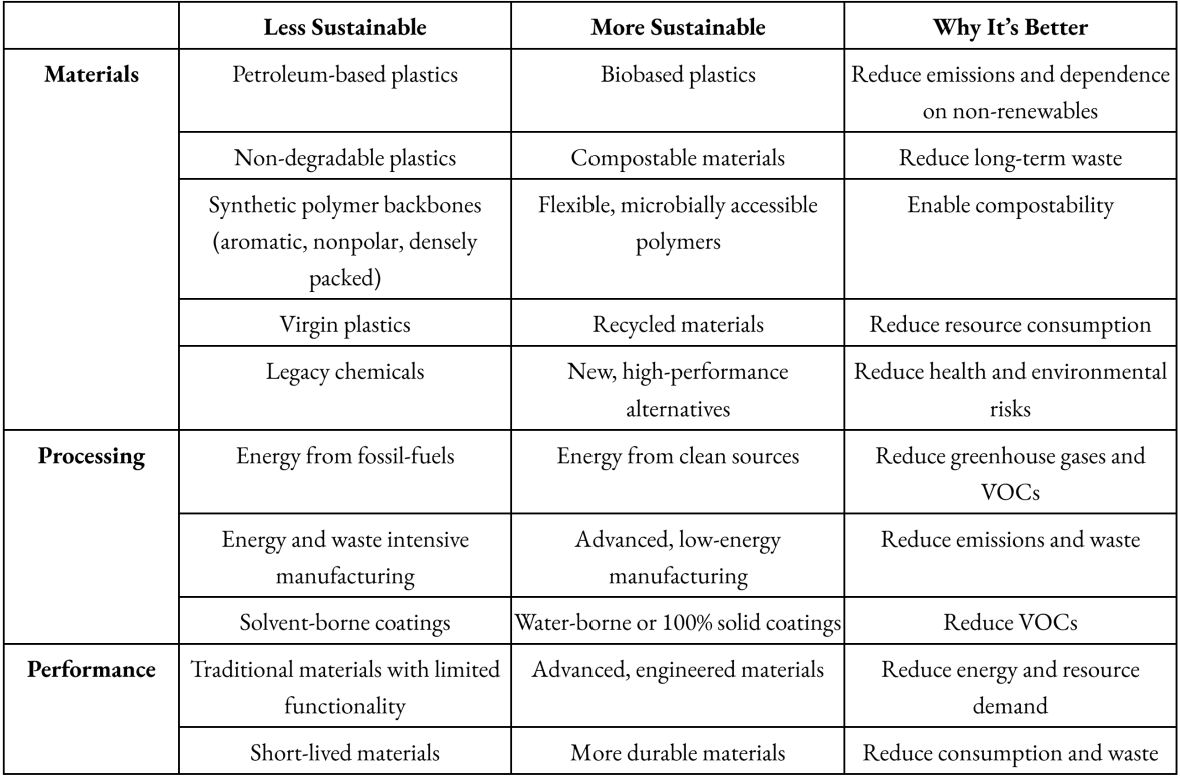
Table 1: A summary of the less sustainable and more sustainable materials, processing, and performance considerations.
Rethinking Materials
Plastic is the most widely produced material in the world today, found in items such as packaging, textiles, fishing nets, and paint. Most conventional plastics are derived from petroleum, and the same chemistries that make them strong, lightweight, flexible, and cheap also lead to their environmental persistence. Plastics are problematic at both ends of their lifecycle: petroleum processing generates emissions that affect climate and air quality while mismanaged waste contaminates land and oceans with microplastics and harmful additives.
These two challenges, emissions and waste, require different material strategies. Production-related emissions can be reduced by swapping virgin petroleum-based plastics with biobased or recycled materials while plastic waste can be reduced by utilizing compostable materials. In some cases, materials can be both biobased and compostable, as shown in Figure 1. To better understand these alternatives, it is helpful to define the terms biobased and compostable.
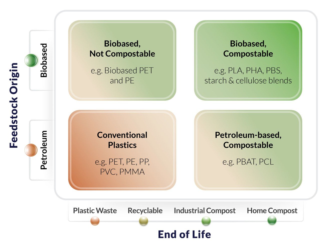
Figure 1. Conventional plastics can be replaced with alternatives that are biobased, compostable, or both. Recycled materials that are derived from petroleum play a role in reducing impact, but significant barriers limit their potential as a standalone solution.
Biobased Materials
Biobased materials are created by turning renewable biomass from plants, bacteria, seaweed, fungi, or agricultural waste into materials that possess similar properties to conventional plastics. During their lifetime, many of these organisms use photosynthesis to turn atmospheric CO₂ into useful molecules. Petroleum-based materials, on the other hand, are created by refining hydrocarbons trapped underground, which contributes new CO₂ to the atmosphere throughout its refinery and transport.
Compostable Materials
Depending on the extent of processing, a biobased material may retain its compostability. Regardless of its origin, compostable materials break down into naturally occurring components under the right conditions, reducing the volume of mismanaged plastic waste that spills into the environment. Some materials can easily compost at home while others require more intense processing at a municipal facility.
Plastic waste can be broken down through incineration, light exposure, or hydrolysis (a water-driven process that cleaves polar molecules). Hydrolysis can be significantly accelerated by microbes with specialized enzymes that digest polymers. While polymers in food waste and lawn clippings readily compost due to microbial activity, only some synthetic polymers (plastics) can undergo microbe-assisted hydrolysis. These microbes can only break down certain flexible and accessible backbone chains that tend to differ from the densely packed, crystalline, non-polar, and stiff backbones that arise from turning petroleum into plastic (Figure 2). Biodegradable or compostable materials are therefore composed of polymers that can be recognized and processed by microbial enzymes. While biodegradable is a non-specific term, certified compostable materials must meet defined criteria for home or industrial composting.
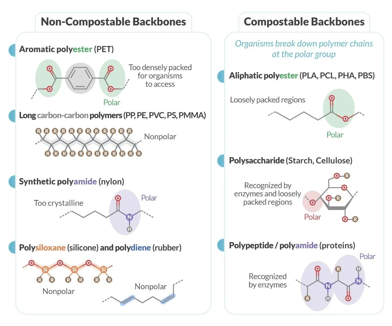
Figure 2. Polymers and plastics (synthetic polymers) consist of long, repeating backbone chains. Select backbones can undergo hydrolysis during composting if the polymer structure, morphology, and environment allows. While organisms can attack polar bonds, they are stymied by non-polar, aromatic, or densely packed crystalline chains.
Other Material Considerations
While polymers make up the bulk of plastic, formulations also rely on a wide variety of precursors, additives, solvents, and colorants that can present significant hazards. For example, fluorinated compounds such as PFAS have been widely used for their durable water-repellent properties, but these “forever chemicals” are increasingly linked to environmental and health concerns, driving their replacement with silicone alternatives. Similar regulatory and consumer pressures have resulted in the phase out of legacy solvents, BPA, heavy metals, and other additives used in plastics. Synthetic dyes and pigments may face a similar trajectory since they contribute to water pollution, require energy-intensive mining and grinding, and complicate recycling and composting. Bio-based dyes and structural color are emerging as a more sustainable option for these traditional colorants.
Rethinking Manufacturing Processes
Another aspect of sustainability is adopting manufacturing processes that minimize fossil-fuel-derived energy and harmful chemical waste. This requires adapting mature infrastructure to handle new materials on existing lines and reworking other processes to be more efficient.
One major opportunity is to switch from fossil fuels to clean energy sources. While energy-intensive metal and glass manufacturers have historically burned fossil fuels to power furnaces, newer hydrogen and electric furnaces drastically cut emissions. Plastic manufacturing processes (heating, moulding, extruding, and coating) already run on electricity, so switching to a clean energy mix can reduce emissions without overhauling existing equipment. The falling cost of solar energy and the geopolitical volatility surrounding the fossil-fuel market further strengthen the case for this transition. Improvements in process efficiency can also reduce manufacturing waste and reduce energy losses due to excess heating and cooling cycles.
Changing the type of polymer coating also makes a difference. Solvent-borne oil coatings are the least sustainable because they are petroleum-derived, release volatile organic compounds (VOCs), and require energy-intensive heating lines to dry. While water-borne coatings reduce emissions, they can still require long drying lines. Solvent-free options, such as LED UV-cured and powder coatings, are often the most sustainable because they minimize both emissions and energy use without compromising performance. Some of these UV-cured coatings can also be engineered to de-ink during recycling, though this has yet to become common practice.
Improving Material Performance
Environmental impact can also be reduced by adopting advanced materials that improve the functionality of existing products and extend their usable lifetime.
Many of these advances improve the efficiency of existing systems. For example, smart window glass like those produced by Tynt Technologies can lower energy demands by preventing buildings from getting too hot or cold, reducing the need for heating and cooling. Similarly, textured light-trapping coatings can increase the power output of solar panels or improve light utilization in agricultural systems, leading to higher crop yields without additional land or inputs.
In other cases, improved material performance can reduce reliance on additional materials or more complex processing. Emerging ink-free labels use structural color to replace dyes and pigments, while also introducing eye-catching optical effects like iridescence. By eliminating inks, these approaches can also simplify material systems and improve recyclability.
Improved performance can also enable safer material substitutions. For example, engineered antifouling marine coatings can replace hazardous metal-based coatings while maintaining performance in harsh environments.
Sustainability Work at SMS
At SMS, we are pursuing multiple pathways to reduce environmental impact through nanopatterning, focusing on materials, processes, and performance.
On the materials side, we have explored lower-impact plastic alternatives, including biobased and industrially compostable films such as PLA and cellulose acetate. These materials offer ways to reduce both production-related emissions and long-term environmental persistence (Figure 3).

Figure 3. Examples of PLA (left) and cellulose acetate (right) nanopatterned films that are biobased and compostable.
From a processing perspective, we have developed nanopatterned coatings that can be applied using a solvent-free, PFAS-free, and UV-curable approach that reduces both energy and material use. The thin, nanopatterned coatings in Figure 4 can be up to 61% biobased, but the chemical modifications that make these polymers robust optical coatings makes them not compostable.
SMS is also leveraging nanopatterning to enhance material performance. By modifying surface structure at the nanoscale, we can introduce new optical and functional properties without increasing material usage. For example, SMS has begun working with customers on vibrant, ink-free labels that create color through structural color rather than pigments or dyes (Figure 3). We have also worked with PowerFilm Solar and MicroLink Devices to develop light-trapping coatings that increase the daily power output of solar panels by up to 10% (Figure 4).
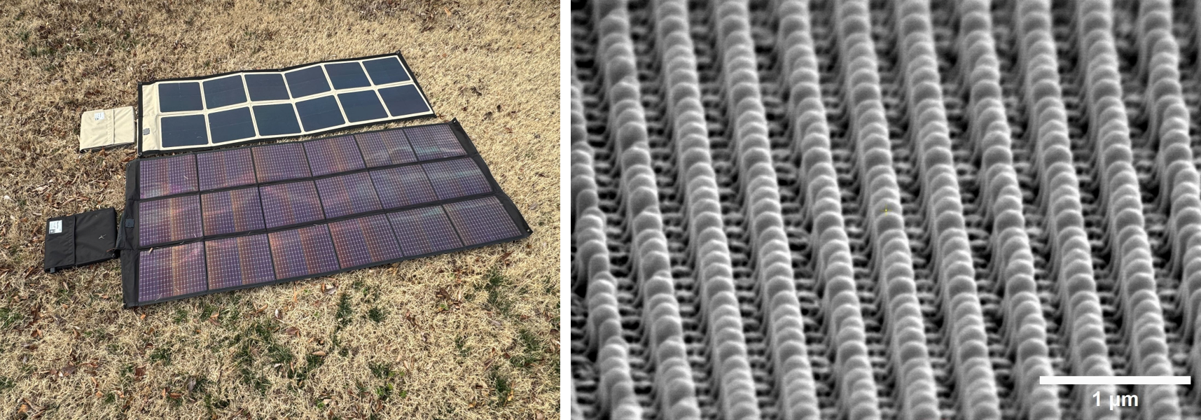
Figure 4. Solar panels that have been enhanced with a 31% biobased light capture coating (left) and an electron microscope image (right) of 54% biobased optical coating.